|
Lechler’s Website: |
|||||||||
|
|
|||||||||
|
|
|||||||||
 |
|
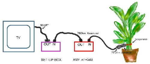
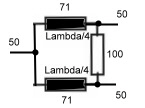
Room plant works as DVB-Television- antenna DVB-terristrical-television is becoming more and more popular. The digitalized TV-signal can be received very perfectly even with little room antennas. If one don’t want to use a technical device as an antenna, a room plant can be used instead as antenna to receive DVB. The plant to be used is the popular dieffenbachia. (don’t touch the sap of this plant).The plant is used as an lambda series resonator with L-coupling: Requirements:
The connection of the plant:
|
|
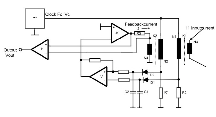
Insulated and potential free DC-current measurement using magnetics. German Patent 3435267C2 Here is a relatively simple circuit to measure insulated DC currents without any DC- loss. Examples for this requirement are:
The primary circuit: We use the well known DC-current measurement method, where a DC current changes the inductance of a coil wound on a core having a hysteresis. The core must be dimensioned in such a way , to change the hysteresis by means of the DC current to be measured flowing only trough one up to three windings on the core. If the temperature never changes and each core would have exactly the same hysteresis , the development would be very simple. But its not the case. We solve this two problems using a feedback circuit witch cancels all unlinearity and outside influences. The circuit used is shown in Fig.1 . We see two controlled inductances. K1 and K2. Each inductance is connected to a AC voltage to be divided by the inductances. K1 is controlled from the measurement current I1 whereas K2 is controlled by an feedback current having a proportional value of I1.The difference DV of the DC voltage from both dividers is amplified and leaded back to K2. Its obvious, DV is kept constant in this circuit even if the core constants or the temperature changes. Fig.2 shows, the loop equations.
Fig.1 Potential free DC-current measurement.
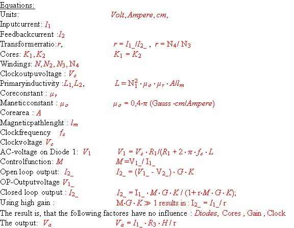
Fig.2 Equations to DC-measurement; DDR Patentschrift 157981 Institiut für elektrische Hochleistungstechnik. BRD Patent DE 343526702 ANT, Siegfried Lechler 1984
|
|
Some broadband transformers using twisted wires 1.0 Basics Broadband transformers to be used in RF-circuits often are build as twisted line transformers where the line is wound around a high permeable ferrite core.The possible transformer ratio is 1. Fig.1 shows the mechanical arrangement on a ferrite bead. Such devices work at 2 Principe’s: #1: At lower band end the transformer works as usual device where the primary inductance certain's the band end frequency fu. Fig.2 shows, the cut off frequency circuit and formula.
Fig 1 Basic transformer #2: At upper band end the transformer works as a line transformer. The ferrite core has no electrical function at band end .The length and the Z of the 2-wireline are the important parameters here. The usual tangents function of 2 pi / lambda is valid here.The transformed Z is : At the length of quarter lambda the well known transformation formula is :
The frequencies between #1 and #2 is the crossing range . Practical transformers never had insertion-loss-ripple there. The crossing of the working ranges is smoothly. The impedance of the wires at Fig.1 depend on the thickness of the copper core, the isolation, and the distance between the wires. It is obvious, that this impedance is unstable. A better practical solution is to twist the 2 wires. The impedance depends here on the number of twists per length. Table 1 shows the impedance of several twisted wires. Tab.1 The impedance of twisted wires
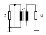
2.0 The auto transformer An other circuit allows an impedance ratio of 4. Fig.3 shows the basic circuit of this twisted wire auto transformer. If the
used wire has an impedance of Zl = 2Z, the output impedance will be 4Z. For the lowerfrequencys , the above shown
formulas are valid.The upper frequency depends on the on the core dimension and wire. The solution then will be always a
compromise between core size and lowest frequency and bandwidth. Fig.4 shows the formulas for the upper frequency
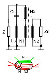
Fig. 4 Fig3. Broadband auto transformer Practical devices of this type my span 3 decades. 3.0 Variable ratios Up to now , we could realize the ratios of 1 and 4 .To match practical circuits , different ratios are necessary. This can be reached in mixing normal design with broadband design. Fig.4 shows this solution having a Z-ratio of 2. As the single winding N3 has low coupling, we must compensate the stray inducdance using a series resonator Cs and Ls. The data is:
Fig.4 transformer having a variable ratio
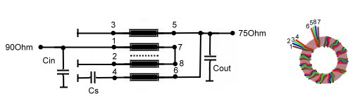
Super broadband transformer matches bit rates. German Patent: DE4302929C1 , DE43029230C1 In high bit rate digital communication systems, components having very broad band transmission are necessary. If we imagine that one bite must not be flattened and make an fourier analysis of one bit, the necessary upper frequency must be about10 times the bit rate . As bit rates my vary from khz to Mhz range a band with from khz to Mhz are necessary in a universal digital modem.The necessary input transformer must therefore cover 4 decades. This values can be reached , using 4 twisted wires, one of them is N3 of Fig.5. but is shorted into the twisting.The series resonator is build inside the transformers windings as Fig.5 shows. The data is:
Fig.5,6 Super performance transformer
|
|||||||||||||||||||||||||||||||||||||||||||||||||||||||||||||||||||
|
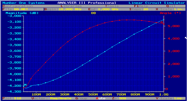
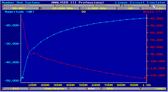
DD circuit linearizes PCB Roll off Due off unavoidable parasistics, RF circuits on PCBs are deteriorated by a roll off up to 1dB. A simple circuit can linearize this roll off. The DD-circuit was developed at the latter days of analog feedback design to differentiate (DD) the signal getting better time behavior, but we will use it as linearizing circuit. Fig.1. Shows a T-circuit having a certain impedance, which is bridged by two capacitors.
Fig. 1 DD circuit The transmission of this circuit depends on its matched Z. Therefore, the reflection coefficients(S11,S22) of the connected devices, must not below 15dB.The Transmission is:
We see 2 corner frequencies producing +20 dB per decade and a -40 dB corner frequency. Adjusting the damping of this corner frequency and the corner frequencies, the circuit can be either a linear, a parable or a ripple function. Fig.1
fig. 2 S12, S11, DD circuit using C1= C2 =15 pF; R1 = R2 = 12 Ohm; R3 =100 Ohm
|
|||||||||||||||||||||||||||||||||||||||||||||||||||||||||||||||||||
|
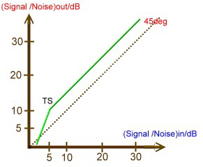
The Noise Threshold of PLL -FM-Demodulators PLL FM Demodulators are widely used in communications receivers, because of its low noise threshold. Below this threshold the demodulator
noise will increase drastically. Fig.1 shows the typical Input Signal to Noise Ratio versus Output Signal
to Noise Ratio diagram of an PLL- FM- Demodulator. Fig.1 Typical noise Threshold of a PLL - FM-Demodulator A very good value of the threshold TS is 6dB.The threshold formula shows, that lower values are difficult to develop. The threshold TS is :
From this Formula, it is obvious, the threshold only can be optimized , by increasing PLL bandwidth and speed. Only using a high order loop will increase PLL speed. |
|||||||||||||||||||||||||||||||||||||||||||||||||||||||||||||||||||
|
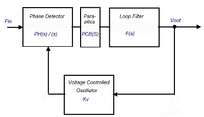
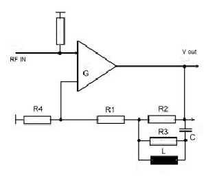
An high order PLL, to be used as an FM-Demodulator, must be made faster than the simple ones. The earning of the bigger bandwidth leads to higher signal sensitivity . In the Literature, one can find first order and second order loop PLL’s. But this circuits are limited especially in the bandwidth of the PLL at the upper bandend. In this demodulator application, the parasitic’s of a PCB will decrease the bandwidth. A way out of this problem is to use high-order filters and increase the total order of the PLL in producing extra phase for loop stability. Fig.1 shows the discriminator circuit. Fin is the FM modulated carrier. The demodulated video signal then appears as Vout.
Fig. 1 PLL
Fig.2 The high order loop filter
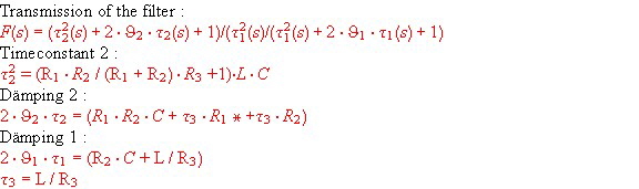
The well known equations for the open loop are: Gain = Kv*Ph(s)*F(s) *PCP(s) .The parasitic of component connections lead to a roll-off PCB(S), this roll off must be compensated by means of the filter :
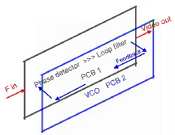
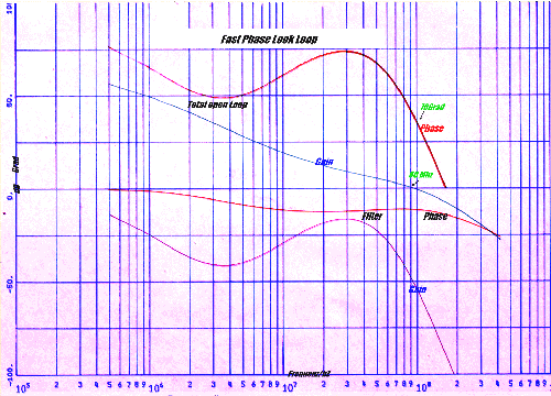
As Fig.1 shows, there is always a low pass of the PCB layout in the signal path. To minimize this parsitics, the best layout of the PLL is a sandwich of two small PCBs where the feedback signal flow is in the opposite direction than the main signal . Fig.3. Fig.4 shows the open loop Nyqiustdaiagram . The zero crossing frequency of the gain is at a frequency of 90 Mhz .Using this Bandwidth, the PLL will demodulate a video signal with a better threshold value than an smaller PLL: The datas are :
Fig. 4 Open loop Nyquistdiagram of a Fast PLL
|
|||||||||||||||||||||||||||||||||||||||||||||||||||||||||||||||||||
|
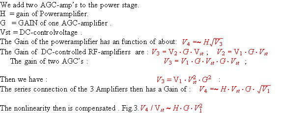
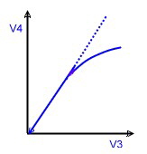
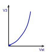
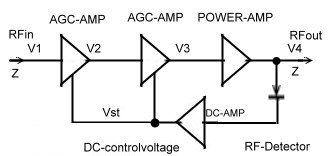
A linearized AGC-Amplifier German Patent DE 3606703C1 AGC-Amplifiers to be used for RF or IF application , have a certain DC- controlled gain range. In this range the amplifier works linear and no distortion must be expected. But to get high RF-power at the output, a power stage has to be added . In this case, the controlled gain rage is limited by the saturation of the RF-amplifier , Fig.1. This limitation will cause intermodulation products especially at multi carrier operation. Do avoid this signal distortions, the amplifier must not work at a working point above 3 db below saturation. Fig.1. This requirement limits the regulation range for the incoming unstable RF signal. With a simple linearisation circuit , the regulation range can be enlarged a lot. The function is as follows:
Fig.1 Power amp. Fig.2 Two AGC-amp’s Fig.3 Total-circuit
Fig.4 New RF-AGC
|
|||||||||||||||||||||||||||||||||||||||||||||||||||||||||||||||||||
|
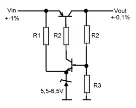
Some RF circuits for instance oscillators, are very sensitive to DC supply variations. This circuits need a DC Voltage of 0,1 % instead the usual 1%. A simple pre regulator solves the problem. Fig.1 shows the circuit. The values of the transistors depend on the main current and the beta of the transistors.The Zener voltage must be selected for maximum stability. The main transistor may be very small, if the big filter capacitors are on the input of the pre regulator to avoid big inrush currents . Fig.1 DC Preregulator |
|||||||||||||||||||||||||||||||||||||||||||||||||||||||||||||||||||
|
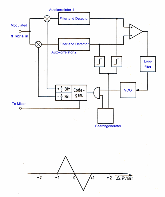
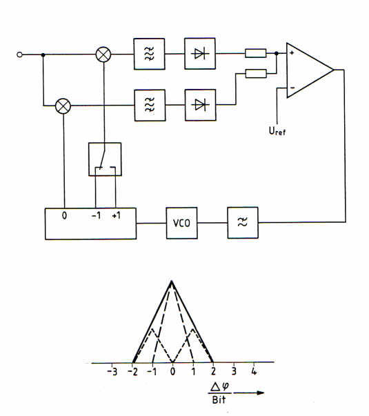
Spreadspectrum AKF has 4 bit range In the telecommunication code multiplex technology, the modulated signal is spread with a codeword. This technique is called spread spectrum. (SPRSP). In a SPRSP receiver the code word must be found and looked to be received. Fig. 1 shows a standard delay look loop to be locked to the code word which has a certain length, for instance 256 bit. We see here a code generator to generate a certain codeword.The code generator is shifted in its phase from a voltage controlled oscillator to be locked in with the incoming, code word. If they coincide, the loop is looked.The shifting of the code word versus the incoming code word has a control AKF-funktion of Fig.2 The linear look-in control range of the feedback is plus minus 1 bite.Outside this control function the loop may flip out and the signal path is interrupted. In Fig. 3 is a new AKF-Loop shown where the lock-in range is twice. The total lock in process is now easier and faster.This broader AKF is reached by summarizing the output voltages of the detector instead of subtracting them and switch the code generator periodically plus minus one bit.
|
|||||||||||||||||||||||||||||||||||||||||||||||||||||||||||||||||||
|
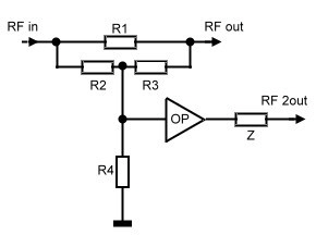
The distribution of RF power in circuits is normal.To realize this power splitting, a lot of practical couplers, dividers ,and splitters are on the market. But at broadband circuits for digital communications their specification are not precise enough. S21 Transmission specification in RF circuits for digital communication are very tight , ripples and roll off must be below 0.1 dB. For instance , the sinx/x increase for a digital radio modulator is only 0.5 dB absolute. Look at: Link >>> Go to digital radio modulator A simple active splitter can divide Power very precisely. Look at Fig. 1 where a doubel-T resistor network is used. An RF. -OP-AMP amplifies the divided power.This splitter may split the signal to a intermodulation feedback system.
The data’s are:
|
|||||||||||||||||||||||||||||||||||||||||||||||||||||||||||||||||||
|
Power dividing and combining is a standard requirement for RF- Designers. The following circuits or components are used :
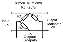
1.0 The Wheatstone Bridge as a coupler. The easiest way to couple a signal in the range from DC to 500 MHz into an other path, is the use of a Wheatstone bridge. The advantage of this circuit is: He is only resistive, has no transformer no complex wiring and is ideal for digital broadband application. But the outputs have no reference to ground. Fig.1 Therefore this bridge is seldom used. At lower frequencies , the 2 outputs can drive a RF-Operational Amplifier . Fig1 shows a circuit and its resistance values depending on the coupling factor a.
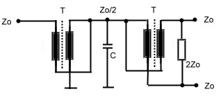
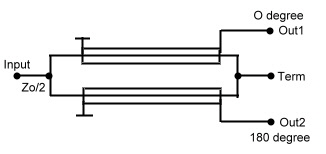
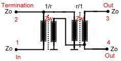
Fig.1 Wheatstone Bridge used as coupler 2.0 Wave Line and Twisted Wire Wave Line Combiners Twisted wire wave line combiners and dividers are realized using a combination of broadband Fig.1 Twisted wire wave line transformer divider/combiner A standard twisted wire wave line combiner is shown at Fig1. Two equal wave line transformers are connected in series. The input transformer matches the power dividing output transformer. This arrangement may be used as combiner or divider. The capacitor compensates the stray inductance’s at broadband applications. This circuit obviously is a three port. Using a simple 1:1 normal transformer realizes a four port device, Fig.2. Here, the transformer will limit the bandwith. A better RF- solution is it, to connect wave lines or twisted wire wave lines in a series- parallel circuitry, Fig.3 .The wave lines at Fig.3 may be replaced by twisted wire transformers, but if the Impedance of the twisted wire is not equal to Zo, phase deviations up to 25 degree will occur. There are many possibilities to build wave line combiners and dividers in a similar manner.
Fig.2 Simple 4 port coupler Fig.3 Paralleled Wave line coupler One classical circuit at low frequencies is the Sontheimer coupler US Patent 3426298 of 1969. Fig.2 Fig.2 Sontheimer Coupler Practical Data’s of Twisted Wire and Wave Line combiners are:
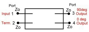
Further readings wave line combiners : R.E.Fisher, “ Broadband Twisted Wire Quadrature Hybrid, “ IEEE Transaction on Microwave Theory and Techniques.” Vol. MTT-21, May 1973 3.0 Line Hybrids Hybrids in general are 90 degree combiner or quadrature couplers Fig.1 One of the two outputs has a phase difference of
90 degree referred to the input port. The fourth port is the isolated port, which must be terminated, but has normally no
power on it. Line hybrids are such 90 degree combiners and are very popular at frequencies in the UHF range.They divide
the input power at port 1 to two output ports 2 and 4, having a loss of >3dB. Therefore they are called “ 3 dB couplers”.
The two outputs have a phase shift of 90 degree. Port 3 must be terminated, to absorb reflected power in case of output
mismatching; normally there is no power at this port.The input port matching therefore is relatively independed of the output
matching.The mechanical construction is very simple.Two lambda/4 lines are coupled by means of a very good delectrica
either in a cable or on a substrate.The mechanical length can be shortened if the lines are meander shaped The dimension of the coupler depends on the epsilon of the dielectric medium. Zo = SQR(Zg Zm).Fig.2
Fig1. Basic Hybrid ^ Fig.2 Line Hybrid Practical Data’s of Line Hybrids are:
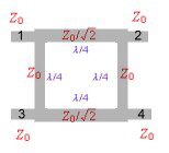
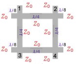
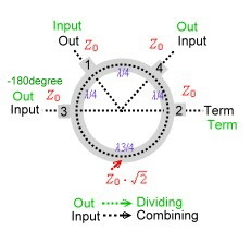
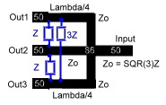
4.0 Brunch Line and Ring Couplers Brunch line couplers are Hybrid couplers related to Fig.1 of 3.0 They have four lambda/4 branches , and are the classical microwave couplers. They are very easy to realize as PCB or micro strip on a substrate. But they have the disatvandiges of low bandwidth, 90 degree phase between the two outputs, a loss of >= 3 dB and big dimensions at frequencies below 1 GHz. Fig.3 presents the mechanical drawing of the classical brunch coupler. Each branch has a length of lamdba/4 .Besides this arrangement other mechanical outlets are possible. If the input and output impedance’s are different , the brunch impedance will be: Zo = SQR(Zin Zout /2): Fig.2 shows a brunch coupler version having Lamba/8 matching stubs on the inputs . A similar microwave coupler is the ring (or magic T coupler, this is a waveguide structure) and is shown at Fig.5. This hybrid may be used as combiner or divider if the inputs and outputs are exchanged. (green = divider, black is combiner.) The phase difference of the output is -180degree. The hybrid transmission is a function of amplitude ratio and phase of the incoming signal.Therefore, to combine signals with an hybrid, they must be matched within a certain percentage in amplitude and phase. Fig.1 Brunch line Coupler Fig.2 Matched Brunch line Coupler Fig.3 Ring Coupler (Magic T Hybrid )
Practical Data’s of brunch line and ring couplers are:
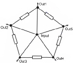
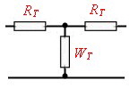
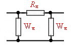
5.0 Wilkinson Couplers Wilkinson couplers or hybrids, are n- port couplers what means, signals on n-ports my either be added or divided. Indeed this coupler is not a hybrid ; therefore all outputs have the same phase of 90 degree related to the input. The basic idea, is a star network of transforming circuits balanced with lumped resistors Fig.1. The transforming networks can be either consisting of L-C-Circiuts or many wave line transformers. Fig. 2 shows a 50 Ohm two port divider and Fig.3 an practical strip line three port arrangement. For higher frequencies the balancing resistors may be a problem an must be induction free and hat sink.
Fig.1 Basic idea Fig.2 50Ohm divider Fig.3 Three port divider For further readings see : ”Microwave Journal Sept. 85 p. 205 Practical Data’s of Wilkinson couplers are:
|
|||||||||||||||||||||||||||||||||||||||||||||||||||||||||||||||||||
|
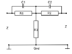
At the old RF Circuits, we matched different components, circuits and amplifiers by designing complicated lumped LC-circuits by means of the smith chart, to not loss any gain of the circuit. As gain is not the problem any more, due of integrated RF Amplifiers, matching philosophy can be changed to resistive compulsory matching. That means, amplifiers and circuits are connected using a regular resistive network having some gain loss. This loss then is compensated by using one or two more amplifiers. The advantage of this method is the total saving of matching-adjustment manpower. But sometimes intermodulation products my be a problem and must be calculated.. Now, remember the resistor networks to be used for matching :
Where alpha is the damping (Neper ). 1 Neper = 8,6859dB Retoure :
|
|||||||||||||||||||||||||||||||||||||||||||||||||||||||||||||||||||
|
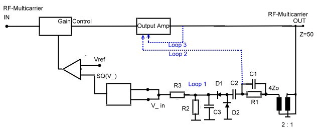
RF multi loop regulator regulates Power This old circuit of the seventies, is shown here as an example for understanding multi-feedback-loops. But the shown Problems of RF. power measurement and intermodulation products are still present today. Simple circuit measures multi carrier power in a RF Power regulator. The output power of a multi carrier RF System, only can be kept constant, if the summ-power of all carriers are regulated by means
of a RF-Power regulator.To regulate this multi carrier power, the RF summing power must be measured, using a prober sensor or circuit. The only true measurement method of RF power
measurement, is the use of an thermal device, for instance a complicated arrangement of an absorber and a temperatur-sensitive resistor (NTC). As this is a complex and expensive
component, and not a high reliability proven component like an integrated circuit, one must find a way to measure the multi carrier power by means of an other methode.The method, I
propose here, is the use of an effective voltage measurement device in series with a DC-multilplicator. As a voltage measurement circuit the voltage doubler, a circuit of the latter
past war electronic days, can be used. The Voltage doupler measures the effective voltage of different waveform’s if properly adjusted. (See Electronics Feb.17, 1961), Using Schottky Diodes as rectifiers, the necessary power level must be about 0 dBm. As a DC- multiplier, an standard
Transconductance OP may be used. Fig. 1 shows a proven measurement circuit in the feedback-path of a 70 MHz RF-power- regulator. As the voltage doubler works best on a
high Ohm source, a broadband transformer is connected to the 50 Ohm RF output. The components C1 and R1 , C2, R2, must be adjusted to get the effective voltage values of carriers
and noise.The gain control voltage V_ becomes :
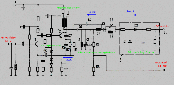
The final multi carrier Power regulator So far, our circuit regulates the multi carrier power, but as it is in electronics, a new problem comes up :. Intermodulation. At an output-level of 0 dB and 20 carries, the two tone intermodulation-product-distance of a small integrated RF Amplifier is only a few dB. Therefore, the only solution seems to be the use of an oversized huge power amplifier. An other solution is a multi feedback regulator which keeps the output power of the carriers constant and suppresses unwanted second and third order intermodulation products. I(1,2) =2f1+-f2 and I(3,4)=2f2+-f1. This products, must be suppressed otherwise the measured RF power is not true. To suppress this products, several LC networks and loops are used. ( L1;C1/L2;C2) Fig 2 shows the total circuit of the RF output..
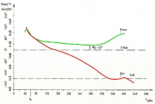
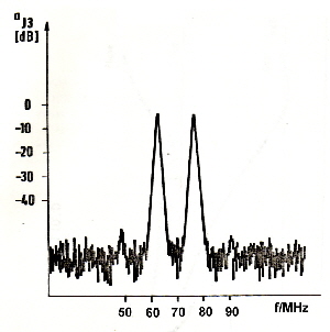
We find here the above mentioned Power detector (D1, D2); which is connected by means of an filter network and a transformer to a classical small power transistor RF amplifier.The output-filter network, suppresses the main part of the intermodulation products.This is the main power loop as shown at Fig.1. This loop has to have at least a gain of 20 dB at the upper end of the band (75 MHz). How this loop works shows Fig.3 where we see a gain of 30 dB at 70 MHz. Minimum Phase is 40 degree which gives a stable device. Now we look again to Fig.2 where we have two more loops 2 and 3 which suppresses unwanted intermodulation products into the output amplifier. This loops control transistor T1 as a basis circuit via a -180 degree signal on its emitter. Although we use a small transistor amplifier, the two tone intermodulation products are 50 dB less the carriers.Fig.4. In case of 20 carriers, this value is > 20 dB.
Fig.3 Open Power loop.
Regulator Data:
|
|||||||||||||||||||||||||||||||||||||||||||||||||||||||||||||||||||
|
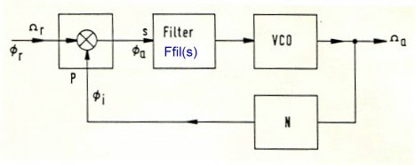
The Loop design of a low noise PLL Oscillator German Patent P3725732.3-35 It is standard, to use a PLL oscillator as a main Clock in communication systems. The PLL oscillator is used because of its low noise and jitter on its outputsignal. A regular unregulated oscillator, beside its main signal, produces noise and jitter too. This unwanted signals may produce bit failure rates and phase problems in the system. Lets look for instance to the phase noise (db/Hz) at a frequency of 10 Hz, of different oscillators :
This article shows a design of a very low noise 10 MHz PLL clock. This clock may be used, as a master clock for a communication system. This design is an example of regulator feed back loop design. Due of its feedback, the PLL can reduce the phase noise values of the PLL components such as mixer, divider and VCO .We start with the block diagram of a PLL oscillator at Fig.1 where the frequency of a Voltage Controlled Oscillator (VCO) is
digitally divided with the counter N and compared in a mixer with a very precise very low frequency standart.The difference-DC and low frequency output of the mixer then is filtered in Fil.(s) and feed as control voltage to the VCO.
Now we need two main equation of the PLL :
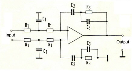
The following circuit design has he goal, to realize a filter, which solves this two main equations to get a stable PLL and a very low noise at the output. Now, how does this goal com out, if we use a standard third order PLL filter ? The remembered circuit of this filter is shown at Fig.2. Fig.2 Third Order PLL Filter
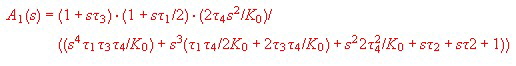
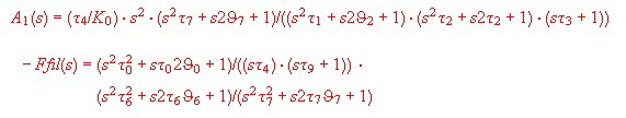
Using this Filter, we get the VCO transfer [2] :
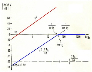
Making a bode plot consiteration[*] we find the rejection of oscillator disturbances at higher frequencies to low. See Fig.4 [*] Go to Bode plod explanation The red line is the gain differentiation (s) at a gain of Ko=1. At the left side of this line , oscillator noise is rejected. Using higher gain we get the blue line for A1(s) and a much better rejection of noise. Yet the gain can not increased to very high values of Ko, due of the stability requirement of equation [[2]. Once more, the filter OP-Amp schould not produce any negative phase angel, this means, one must use standard OP-AMP’s having a 10 MHz bandwith.
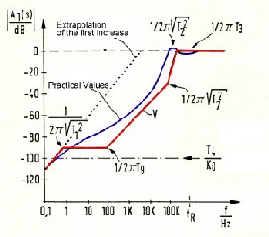
Obviously, distortion frequencies above 100 Hz can not be rejected. We see, this filter is not very useful in this application. Now we construct us a better rejection, starting with Fig.4 using new corner frequencies and get the red line of Fig.5 Fig.5 Construction of a better noise rejection (red)
If we could realize this diagram with a practicall filter, distortions up to a few100 kHz could be rejected. The question now is, how does the new filter has to look like. It is obvious, the basis filter is the filter of Fig .2, but we need three more corner frequencies.The formulas to get the red curve of Fig.5 can be written as::
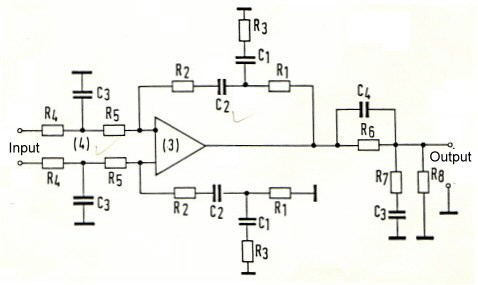
After trying and working for a while, we find the filter circuit of Fig.6 . Fig.6 The new PLL filter
As we have only roughly constructed the bode diagram, we have to check the result using a computer using the values of: The result of the computer run gives the following corner frequencies if the reference frequency is: fr = 1 Mhz:
The rejection transfer is the blue line at Fig.5. Yet the computer can check stability too, and we find the loop very stable as Fig.7 shows.
Fig.7 Stability of the PLL, using the new filter. Readings:
|
|||||||||||||||||||||||||||||||||||||||||||||||||||||||||||||||||||
|
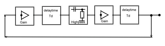
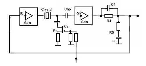
Watch the dead time in simple Crystal Gate Oscillators ,(A feedback example) A simple crystal IC-Clock using digital components, must be analysed properly, otherwise this clock can make lots of trouble in producing noise and jitter and discrete frequencies. If we use two simple NAND Gates in series, as loop amplifiers, we get very high loop gain, but high delay time too. The phase of this dead time jumps continuously between 180 and -180 degree up to highest frequencies. At this frequencies, the gain must be -10 to -20 dB and the phase must have a distance of minimum +30 degree from zero. Otherwise the Clock will produce a lot of noise. First, we analyze a simple oscillator circuit using digital gates as Amplifiers and find 4 Feedback blocks at Fig.1
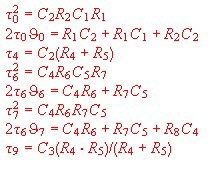
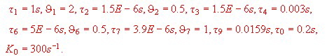
Fig.1 Blocks of a simple gate oscillator Summarizing the data’s of the NAND Gates gives the following Values:
Fig.2 Analyzing a digital Gate Oscillator
Fig.3 Crystal oscillator with dead-time compensation, using digital gates.
|
|||||||||||||||||||||||||||||||||||||||||||||||||||||||||||||||||||
|
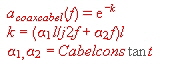
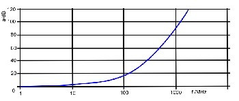
Watch this tiny miniature Coaxial Cable In complex communication units the interconnections of RF signals, are realized by means of small very thin coaxial cables, having a length of only a few centimeters. But this small pieces of cable my be the source of an unwanted roll off. Therefore, watch the quality of this “unimportant “ cables, before installing it. A rule of thumb equation to get the loss of a coaxial cable per meter is: [dB, Hz, meter]
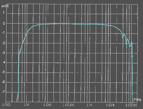
Fig.1 Typical coaxial cable roll off . This two constants define the bandwidth of the cable. Fig.1 shows a typical roll off at a certain length of a miniature coaxial cable. The corner frequencies of the roll off depends on the two constants and the length. A short transmission measurement of the used inter wiring cable including tiny coaxial connectors, clears the problem . An universal Nonlinear OP-AMP, German Patent DE3216707 C2 Nonlinear OP-AMP’s are very usefull at many applications:
With the classical non-linear circuits several biased diodes are used in the feedback of an OP. As this circuits are difficult to adjust, or not adaptable, for RF- filter tuning, another circuit was invented in 1984. As Fig.1 shows, the feedback paths are switched using FET- switches for different Gains.This are are simple resistor feedback paths. The switches are switched, using an analog digital converter. Using adapted feedback resistors, we can realise any nonlinearity to the application.The formulas, are very simple as Fig 3 shoes. Fig1,Fig.2,Fig.3 Nonlinear opamp circuit. Well matched RF-Amplitude-Equalizer German Patent DE 3542655 C1 To compensate for ripple amplitude due to the mismatch or losses in RF circuits, various amplitude equalizer circuits are known.Unfortunately, most of them have a high input and output reflection and and relatively high losses. The new Amlitude equalizer is good matched and has a low beginning loss. Typical Datas are:
Fig.1 shows the circuit and Fig.2 The typical damping
Fig.1 The new amplitude equalizer Fig.2 Typical slope
Typical Values in the 140MHz IF-range are:
|
|||||||||||||||||||||||||||||||||||||||||||||||||||||||||||||||||||
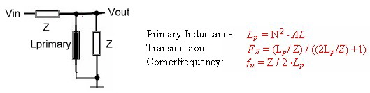
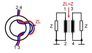 Fig.2 The lower band end
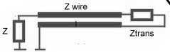
 wave line transformers. Due
of the used technique they are restricted to relatively low frequencies, but they have the advantage to be very broad banded and very small
in size. It is therefore sometimes desirable to realize such a combiner for high frequencies up to 1 GHz. This becomes clear, if one
compares the size of an 3 dB strip line coupler having a dimension at 1 GHz of 7*7 cm, with the 0.5 cm square of a twisted wire combiner.
wave line transformers. Due
of the used technique they are restricted to relatively low frequencies, but they have the advantage to be very broad banded and very small
in size. It is therefore sometimes desirable to realize such a combiner for high frequencies up to 1 GHz. This becomes clear, if one
compares the size of an 3 dB strip line coupler having a dimension at 1 GHz of 7*7 cm, with the 0.5 cm square of a twisted wire combiner. 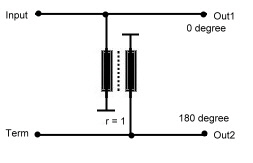
 In this hybrid, we have two impedance’s, the mutual
impedance between the two lines Zm and the impedance’s from the lines to ground Zg. The coupler input impedance then is :
In this hybrid, we have two impedance’s, the mutual
impedance between the two lines Zm and the impedance’s from the lines to ground Zg. The coupler input impedance then is :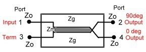
 The transfer of this filter is :
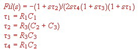
 and :
and : 
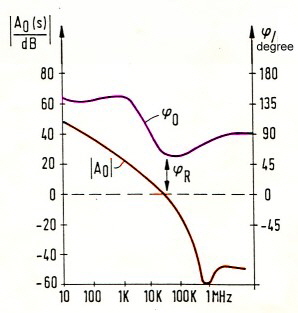
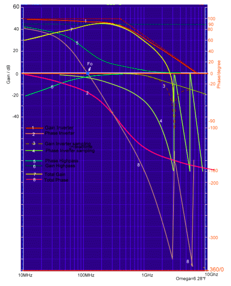 To analyze the oscillator, we draw the
standard transfers #1 to #8 into the bode plot of Fig.2 and find the zero Phase at maximum Gain of about 20 MHz at Fo. This is the
Frequency the Oscillator will run. We see, that this frequency is dependent of many unstable Parameters of the NAND gates, which are
not specified as an analog device. For this reason, a crystal will be connected in series to the high pass. The second problem we can
see now, is the Gate Dead (delay) Time (3,4). The Phase of the dead time, jumps at twice its frequencies 1/Td to A Phase of -180 degree.
Due of this jumps, the Oscillator may run at many higher frequencies too and produce a lot of noise and jitter. This would increase the bit
failure rates in digital communication systems. Therefore, a Phase compensation circuit is build in, to prevent frequency oscillation due
of delay time. Fig.3 shoes the designed Oscillator to be used as an VCO in a communication PLL Clock.The Circuit around C1 and C2 is a standard phase correction
Network and reduces high frequency noise and jitter.The values of C1 and C2 are only 1 to 5 pF. The frequency of the crystal is slightly
changed, using the series shunt Cs by means of a FET transistor. Its resistance value is changed from the DC feedback voltage. The
Crystal itself works in the High Q series
mode
, at its resonance. But at higher frequencies, the crystal works in the parallel mode so that the feedback situation is similar to Fig3.
To analyze the oscillator, we draw the
standard transfers #1 to #8 into the bode plot of Fig.2 and find the zero Phase at maximum Gain of about 20 MHz at Fo. This is the
Frequency the Oscillator will run. We see, that this frequency is dependent of many unstable Parameters of the NAND gates, which are
not specified as an analog device. For this reason, a crystal will be connected in series to the high pass. The second problem we can
see now, is the Gate Dead (delay) Time (3,4). The Phase of the dead time, jumps at twice its frequencies 1/Td to A Phase of -180 degree.
Due of this jumps, the Oscillator may run at many higher frequencies too and produce a lot of noise and jitter. This would increase the bit
failure rates in digital communication systems. Therefore, a Phase compensation circuit is build in, to prevent frequency oscillation due
of delay time. Fig.3 shoes the designed Oscillator to be used as an VCO in a communication PLL Clock.The Circuit around C1 and C2 is a standard phase correction
Network and reduces high frequency noise and jitter.The values of C1 and C2 are only 1 to 5 pF. The frequency of the crystal is slightly
changed, using the series shunt Cs by means of a FET transistor. Its resistance value is changed from the DC feedback voltage. The
Crystal itself works in the High Q series
mode
, at its resonance. But at higher frequencies, the crystal works in the parallel mode so that the feedback situation is similar to Fig3.


|
|