Lechler’s Website:
Electronic equations2 content :
- Basic linear feedback equations
- Computing the transfer of regulator blocks
- Regulator behaviour Standardization
- Regulator and Feedback Filter Blocks
- The Definition of Analog Active Filter Blocks
Basic linear feedback equations
Feedback is everywhere where electronic circuits are. A good basic unterstanding of feedback helps to solve electronic feedback problems, having special requirements as:
- AC and DC voltage stabilization
- Operational Amplifiers
- Active filters
- DC-stabilisations of RF-amplifiers
- Automatic gain control, AGC
- Intermodulation products cancelation , IPC.
- Phase Look Loops, PLL.
- Industrial control electronics
1.0 The linear regulator block diagram
Each linear regulator can be simplified to look like the block diagram of Fig.1. The control block Ks and the feedback block Kr. Ks
may be a machine; a power device or a frequency mixer. Kr is the feedback amplifier including phase and offset networks. Fig.1 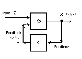 This is the basic schematic of each regulator.The input Z is the unstable value which has to be regulated. The
output X is the stabilized value of Z. Then there is the feedback path which controls Z via the control value Y. The input value Z can be a voltage, a frequency , the speed of a machine, a.s.o.The
control value must not be the same type a the Z value. But can be a voltage, a frequency, a current or a digital byte.
This is the basic schematic of each regulator.The input Z is the unstable value which has to be regulated. The
output X is the stabilized value of Z. Then there is the feedback path which controls Z via the control value Y. The input value Z can be a voltage, a frequency , the speed of a machine, a.s.o.The
control value must not be the same type a the Z value. But can be a voltage, a frequency, a current or a digital byte.
Fig.1 Basic regulator schematic.
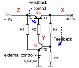 Fig. 2 Simple voltage regulator.
Now, we look to the circuit of the simple DC voltage regulator of Fig.2. Transistor 1 is the control block, transistor 2 the feedback amplifier. The Input voltage is Z, the output voltage X. The base current of T1 is the control value Y. If the input voltage does not change we have a stable balanced condition, which is inticated by this big letters, X,Y, and Z. But this values may change if the input Z changes a small amount dz. The other values then will have the deviations dx and dy. This deviations are considered very small. compared to the stable condition values.
Now we divide Ks into two blocks, one for the input and an other for the controlling and get a new but more detailed schematic.Fig3
Fig.3 Basic regulator schematic to compute feedback formulas.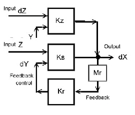
We get a new block Kz which is indeed the block Ks having at the input the deviation dz of Z. But has an fixed control value Y , the outcome of a certain stable condition. At Ks it is vice versa. We led the input Z be the stable value and the control value have the deviation dy. The feedback regulator gets a new external control input W to control X via the adjustment dw. To get am more detailed equaition, we look again to the simple regulator of Fig.2 and see in the feedback the resistotors R1 and R2. This are the measurement resistors for the feedback whereas the zenerdiode adjustes the output and is W. In regulators the measurement often is frequency depentend we get a additional block Km. Km is part of Vo and must be consitered computing Vo. Yet we can find the main regulator formulas :
2.0 Behavior to input deviations dx/dz
- dx/dz = Kz / ( 1-KrKsKm).
- KrKsKm is total loop gain ; Vo = KrKsKm .
- It is obvious, that V must be a negative value to get regulation, we get:
- dx/ dz = Kz / (1+Vo) ;
3.0 Behavior to external control adjustment dx/dw
- dx/dw = -KrKsKm/(1-KrKsKm)
- dx/dw = Vo / (1+ |Vo|)
- If Vo >> 1; dx = dw.
- Regulation quality depends on Vo .
- As no regulator is perfect the output X will not exactly follow the external control W:
- The deviation of X due of dw is dxw, dxw/dw = -1/ (1+|Vo|)
The deviations dx, dz, and dy. have been considered to be very small . Yet we must distinguish
between two kinds of deviations. Either small jumps in a certain short time , having the value dz = z![]() ore small sinusoidal voltages having a certain frequency. dz = dz
ore small sinusoidal voltages having a certain frequency. dz = dz![]() . The time jump will
produce another jump x
. The time jump will
produce another jump x![]() and the frequency will produce the same frequency but with an other
amplitude dx
and the frequency will produce the same frequency but with an other
amplitude dx![]()
Using s = ![]() the feed back formulas becomes :
the feed back formulas becomes :
4.0 Behavior to Frequency input Deviations dz(s)/dx(s)
- dx(s)/dz(s) = Kz(s) / ( 1-Kr(s)Ks(s)Km(s)). [1]
- If Kr(s)Ks(s) = Vo(s) >> 1 ; dx(s)/dz(s) = Kz(s) / Vo(s)
Fig.4 Measurement Block Mr
5.0 Behavior to external Control Deviations dx(s)/dw(s)
The Formula then becomes
- dx(s)/dw(s) = -Vo(s) / (1+ Vo(s))
- dx(s)/dw(s) = 1 / (1-(1/Vo(s)) [2]
- If Kr(s)Ks(s)Km = Vow(s) >> 1 , dx(s)/dw(s) = 1;
This makes it clear, to the loop gain has to be as high as possible.
6.0 Transmission Definition of Regulator Blocks
The Gain or Ks(s) or Kz(s ) is expressed as transmission gain :
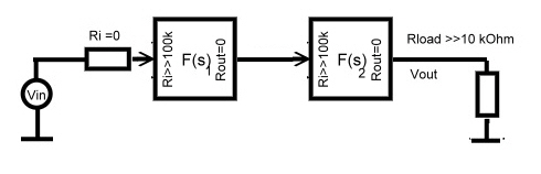
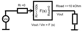 . The input of the driving source is zero and the load resistance is infinite.This is true for low
frequency OP-AMP circuitry.
. The input of the driving source is zero and the load resistance is infinite.This is true for low
frequency OP-AMP circuitry.
Fig.4 Definition of F(s) [Gain] for feedback design
As the main regulator equations are expressed as function of the frequency it is obvious, that to work with and design a feedback circuit, means to analyze and compute equations like F(s). To ease this work we express F(s) in terms of multiplicands to ease the writing of a computer program and to work graphically in a bode plot.
![]()
The multiplicands M1 to M5 are standard expressions and can exist in n numbers.
7.0 The Logarithmic Frequency diagram (Bode plot)
In the Bode plod or an equivalent computer program, the multiplication at F(s ) changes to addition of gain in dB and addition of phases in degree:
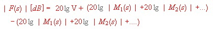 Gain :
Phase: 
The Multiplicands are:
- V = Gain
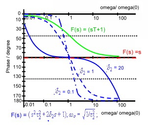
- M1 = First order :
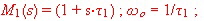
Bode plot values of the denominator: Gain = -20 dB/Dekade . Phase = 0 to -90 degree
Bode plot values of the numerator : Gain = 20 dB/Dekade . Phase = 0 to 90 degree
- M2 = Second order .

Damping : ![]() < 0.8 = Gain overswing
< 0.8 = Gain overswing
Bode plot values of the denominator: Gain = -40 dB/Dekade . Phase = 0 to -180 degree.
Bode plot values of the numerator : Gain = 40 dB/Dekade . Phase = 0 to 180 degree.
- M3 = Integrator or Differentiator: .
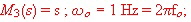
Bode plot values of the denominator: Gain = 20 dB/Dekade .Phase = -90 degree, Integrator
Bode plot values of the numerator : Gain = 20 dB/Dekade .Phase = 90 degree; Differentiator:
- M4 = Dead time term:
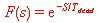
Bode plot values of the denominator: Gain = 0 ; Phase = 0 to -90 degree. -57,3 degree at omega = 1/Td
Bode plot values of the numerator : Gain = 0 ; Phase = 0 to 90 degree. 57,3 degree at omega = 1/Td
- M5 =

The bode diagram of M1 to M3 low pass behavior, shows Fig.5,6:
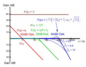
Fig.5
Fig.5 Bode plod of factors M1, M2, M3 Low pass behavior
Fig.6 Phase of factors M1, M2, M3 Low pass behavior
8.0 The time behaviors of regulator Blocks
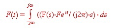
The jump (time behavior) dz = z![]() can be computed using complex integration of F(s) :
can be computed using complex integration of F(s) :
Another solution is the use of related standard time tables or a software, referred to a certain F(s)
See: F. Frauenberger , Regelungstechnik Teubner Verlag 1967.
Better is to use a linear circuit analysis like LISA to compute the time behavior of circuits.
In case of known time behavior the frequency behavior can be computed using Laplace transformation:![]() or use Laplace transformation tables or software.
or use Laplace transformation tables or software.
The above equations are the basic equations to design a feedback. Besides the two design goals , regulation quality , and control quality, feedback stability is the primary goal. As we have seen, in equation [1] and [2] the gain Vo should be very high.(20 to 50 dB is normal). and must have a negative Phase of -180 degree. As he phase of the gain versus frequency will change an other negative angel of -180 degree may exist at a certain frequency. At 360 degree ,the result will be an unwanted oscillation or only an enhancement of noise and jitter, if the loop still has gain. The following limits are valid to get feedback stability in a linear feedback :
9.0 The Stability rules for simple linear feedback
The computed frequency behavior of overall open loop gain V must be in the following limits to prevent oscillation:
- Phase of Vo(s) at the frequency of crossing 0 dB gain : Ph(0db) = 20 to 60 degree
- Gain of Vo(s) at the frequency where the angel is -180 degree (total phase than would be 360 degree): G(-180) = -3 to -20 dB.
- Gain versus frequency of Vo(s) must cross the 0 dB line very flat.
- Gain of Vo(s) must be very high at the maximum regulation frequency or speed.
10.0 How to use a linear circuit anlaysing (LISA) Program to optimize feedback loops and regulators
We have seen the feedback equations 1, 2 and F(s) , are mathematical formulas, containing the data’s of the regulator itself. But parts of the feedback, for example mixer gain transmission , feedback amplifiers, filters and sensors , must be designed as circuits. Therefore , to design a critical feedback , a mix of a mathematical program and a LISA (linear circuit analysis) program is necessary. One can use the following Prog-Cad (Combination of mathematical programs and linear circuit analysis ) to optimize regulators:
- Write a mathematical program for the regulator formulas using C+ or FORTRAN
- Let the results be written into a touchstone S21 file, fitting into a linear circuit analysis)
- Make a circuit file for a S (or Y,or GAIN) parameter Block containing the computed data’s , which is matched on the input and output to match the S-Block, as F(s) like Fig. 4 . Fig.7
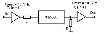 Fig.7 Matched S-Block
- Add this S- parameter circuit to the regulators analyzing LINA (linear circuit analysis, for instance “ Analyser Pro.... Number 1 Systems” ) circuit file.
- Change Parameters in the FORTRAN program and see how the results fit to total circuit running LINA and vice versa.
This ProgCad method allows too, to design the feedback of regulators in the time domain using time CAD programs like LINA for circuits.
11.0 Examples of feedback. Links to :
>>>Goto to the example of DC current regulator
>>>Go to the example of power stage transmission F(s)
>>> Go to an example of regulator open loop
>>>Go to an example of a PLL feedback filter
>>> Go to an example of RF Multiloop regulator
>>> Go to example of PPL Oscilator loop
Regulator Behaviour Standardization
The kind of transmission in a regulator circuit or a regulator block is standartisized to get a fast overlook of regulators behavior and quality.
We distinguish in the subject of regulators between :
- DC and low frequency gain.
- Low pass behavior.
- High pass behavior.
- 1 pole at zero, this is called the I (Integrator) behavior of a regulator
- 1 Pole at infinite, this is called the D (Differentiator) behavior of a regulator
The definition of standartisation is:
- The DC and very low frequency gain is called the proportional behavior “ P ” of a regulator.
- Low pass behavior and Integrator are roughly called “ I ” behavior of a regulator.
- High pass behavior and differentiator are roughly called “ D ” behavior of a regulator.
Now we look to the behavior of a regulator output, if the input z has a time jump z![]() in case of different behavior P, I or D, of the regulators equation:
in case of different behavior P, I or D, of the regulators equation:
dx(s)/dz(s) = Kz(s) / ( 1-Kr(s)Ks(s)Km(s)).
At Fig.1 the typical output x![]() is shown of different regulator equation types after a jump in the input..
is shown of different regulator equation types after a jump in the input..
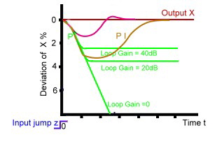 Fig.1 Time behavior of regulator types
In case of only P type (green),), the output X will never reach his old value. This is the steady state P deviation. In case of I type (brown), it takes a long time until the old value of X is reached again. But this I regulator type has at least no deviation at all. Therefore PLL’s which regulate frequencies, always are PI types of regulators. As I types need a long time to regulate, a D Type is added. (violet). But as it obvious, if not properly adjusted, the output may have some over swing. .A typical example of a regulator that needs an optimum time behavior is an elevator.
Computing the transfer of regulator blocks
Beside lumped element active filters, which are prescribed in in many filter catalogue’s,( use the internet search keywords: “active RC-Filters ” ), a lot of R-C-L filters and circuits are needed at analog electronics.The transfer of such circuits is easy to calculate, using voltage divider technique with resistors. Example 1 shows how to do it:
The transfer of the circuit of Fig.1 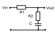 will be computed. We use resistors R and complex resistors L(s) and 1/ C(s), and divide the voltages:
Vout / Vin = F (s) = ![]()
Now we must simplify this equation into a bode plot formula to get a rough idea what the roll off will be :
Fig.1 Low pass network
![]() . Yet we see, we have 2 corner frequencies and two
slopes, -20dB and +20dB per decade and +90 and -90 degree of phase. The precise values can be found using a CAD-program like No.1 Systems ““Analyser” or a graphically bode standart.
. Yet we see, we have 2 corner frequencies and two
slopes, -20dB and +20dB per decade and +90 and -90 degree of phase. The precise values can be found using a CAD-program like No.1 Systems ““Analyser” or a graphically bode standart.
An similar easy way of computing circuits connected to OP-Amps is used in example 2: If we have a simple input and simple feedback network around an OP-Amp, only the the shorted circuit of the input and feedback resistors must be calculated to find the voltage transfer. As we have seen, the resisters may be complex too. Fig.2 shows the way of looking into the networks using the red dotted lines.
.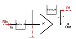 The Voltage transfer becomes:
 ![]()
This is valid if the corner frequency of the OP-Amp is higher then about 10 times the working frequency.
Fig.2 Resistive Networks around an OP-Amp
Regulator blocks may be series or parallel connected . The total transfer of series connected regulator blocks is simple: F(s) = F (s1)F(s2)F(s3).......F(sn) Fig.3. Whereas the parallel connection is difficult to compute and very seldom used. See Elektronik (German) 1973 Heft 6
Fig. 3 Series connection of Regulator blocks
Regulator and Feedback Filters Blocks
As new designed electronic regulators in most cases are instable, phase correction networks must be used to reduce negative loop phase to reduce oscillation. Often a very small circuit will do the job, but some regulators, as noise free Phase Look Loops, need a complicated electronic filter network, to be stable and reduce noise. In this chapter several simple and complicated loop filters are shown. The shown circuits I have used for years in many feedback circuits to optimize stability and time behavior. Some of this circuits are well known, others are not.
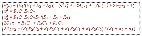
The definition of a regulator block transfer is defined as: ![]() .(or M(s))
.(or M(s))
The given formulas itself are first or second order types:
Description of Regulator Blocks can be found in this Site at:
--------------------------------------------------------------------------------------------------
#1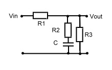 Filter Block : Low pass-Circuit with load.
This Circuit may be used, to stabilize a regulator and decrease regulators speed.
The Transfer is :
Fig.1 Low pass Circuit with load
#2 Filter Block : low Pass Circuit and OP-AMP
This circuit may be used, to stabilize a regulator and decrease regulators speed. The transfer is :
![]()
![]()
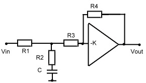
Fig.2 Integrating Circuit and OP-AMP.
#3 Filter Block : First Order High Pass-Circuit
This high pass circuit may be used, to optimize regulator speed and time behavior
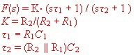 Fig.1 Differentiating circuit equations
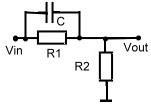
Fig.3 High pass (D) circuit
#4 Filter Block : Second Order High pass-Circuit
This differential circuit (D) may be used, to optimize a regulators speed and time behavior. It also can be used as an RF-roll off --linearizing circuit.
 Fig.1 Second Order High pass equation
 Fig.2 Second Order High pass circuit
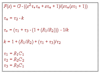
#5 Filter Block: Regulator Behavior Optimizing Circuit
This is the classical circuit to optimize regulator time behavior for industrial process regulators.
(PI D types). As high pass and low pass behavior of a loop filter can not optimize a regulators time behavior and regulation quality, the loop must have an integration behavior, what means one pole at zero F( s ) = 1 / (s) .Whereas the D part may be realized by means of a simple highpas.
Now look at circuit of fig 1. The DC: gain goes to infinite, the D part is realized using C2 and the I part is realized by means of C1.
 Fig.1 Loop filter for regulator PID optimization
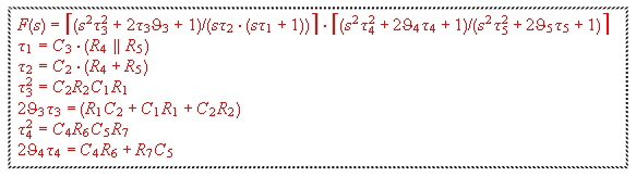
The transfer formula is:
- Index v refers to the D part
- Index n refers to the I part
 |
#11 Filter Block : Positive phase circuit and Roll off circuit for digital Modulators
Filters in digital modulators must have an roll off and a gain overswing.The circuit of Fig.1 can realize roll off and overswing. As both corner frequencies are equal, it also can be used to produce positive phase in a regulator feedback. The earning of positive phase is the result of different damping factors.
The transfer formula is:
Fig.1 Formula for digital modulator filter
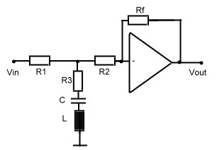 Fig.2 circuit for digital modulator filter
#12 Filter Block : Phase correction circuit for linear voltage regulators
As today’s power transistors are very fast., the loop gain of linear transistor voltage regulators decreases very fast at high frequencies. (More than -40 dB/ Dek.) The result is high frequency oscillation of a simple voltage regulator. A phase correction network must be used therefore.To get stability, the feedback gain must be decreased, by means of an -20dB/Dek slope, until stability is reached. Fig 1 shows the classical circuit. It is important, that the supply voltage is blocked for higher frequencies [MHz range].
The transfer is :
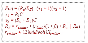
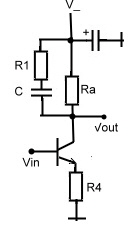 Fig.1 Phase correction circuit for linear voltage regulators
#13 Filter Block: Loop Filters for Phase Look Loops
The kind of a filter to be used in a PLL Loop, depends on the requirement of the PLL. Therefore PLL- filters may either be very simple or complicated. Certainly their transfer is not the transfer of the closed PLL loop. PLL filters may be sorted as follows:
Kinds of PLL- loop -filters:
As phase look loops are used in different applications, their loop filters are different. general there are:
- 1 Order Filter
- 2 Order Filter
- 3 Order Filter
- High order filter for PLL-oscillators.
- High order Filters for PLL-demodulators
First order PLL loop filter
Fig 1 shows the loop filter for the seldom used first order PLL. The Transfer equation is: ![]()

Fig.1 First order PLL loop filter
Second order PPL loop filter
Fig 2 shows the standard loop filter used in a second order loop.Theoretically the low pass consisting of C1 and R1 theoretically is not necessary, but practically, high frequency spikes from digital circuits must be decreased to not latch the OP-AMP. If the OP-AMP is t10 times faster as the maximum loop frequency, the transfer equation becomes:
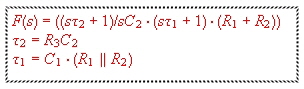 |
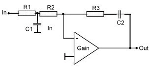
Fig.2 Second order PLL loop filter
For further readings look to : Microwaves May 1985 p 122
As we can see, the OP-AMP for this filter works with maximum Gain, not having a feedback
resistor.This leads to minimum output frequency deviation .. But unfortunately, RF OP-AMPs, need a limitation of Gain using a feedback resistor Fig.3. Under this condition, the second order
loop filter- transfer becomes only : 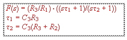 Unter this condition
,the regulator is not optimized.
Unter this condition
,the regulator is not optimized.
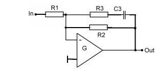 Fig.2 Loop filter with fixed OP-gain
Third order PLL loop filter
The third order PLL loop filter is almost the same as for a second order filter. Fig.3 .
The Transfer is :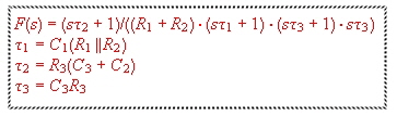
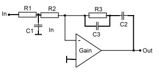
Fig 4 Third order PLL loop filter
For further readings look to : Electronic Design May 197?
PLL Oscillator loop filter
To reject unwanted signals in PLL oscillators, a complex loop filter is necessary. Especially if the Oscillator is used as signal source in digital communications, jittering of bits must be prevented.
Fig.5. shoes a filter circuit to realize a clean PLL oscillator. Its an example of series connection of multiplying transfer of regulator blocks.
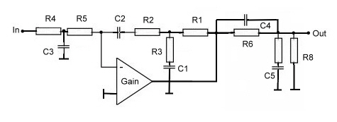
Fig.5 Loop Filter for a PLL main Oscillator for digital communication
The transfer formula is:
Further readings and explaining :
- Bundesrebuplik Deutschland Patentschrift DE 3725732 C1 1987 ANT - S.Lechler, Elektrischer Schwingungserzeuger
PLL Demodulator loop filter
PLL’s at FM-Demodulators have to be very broadbanded. A use full filter to gain stability at high frequencies is shone in Fig,.6. The filter transfer is :
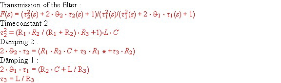
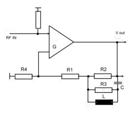
Fig.6 Loop filter for PLL FM Demodulators
Further readings:
- United States Patent 3,611,168 F.Haggai Threshold Extention Phase Look Loop, 1971
#14 Filter Block’s using RF OP-AMP’s
As it was clear, if the OP- AMP has a much higher upper frequency limit than the working frequency, the transfer of the shown circuits behaves like its equations. Yet at RF frequencies, one always are working on the upper frequency limit of OP-AMP’s. Therefore, classical active Filters, will not work proberly. But in case of no filter circuit elements in the feedback of an OP -AMP, only the roll off of the amplifier, may decrease the filter behavior.
Here are several Filters useful at RF frequencies:
Second Order Low Pass
One could think, that the circuit of Fig.1 is a only a low pass, but its an quadratic high pass at the same corner frequency than the low pass , having an other damping. The values of the resistors are responsible for the difference of the dampings. Fig.2
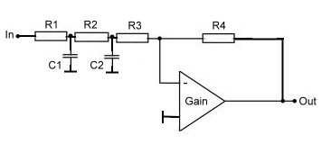 Fig.1 Low Pass on RF OP-AMP
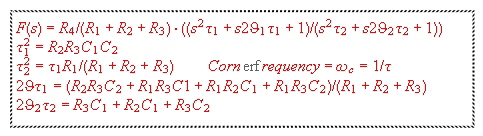
Fig.2 Transfer of the circuit at Fig.1
High Pass and Low Pass
This circuit may be used as high or low pass circuit to correct the loop gain of a regulator.
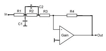 Fig.2 Phase Correction network on a RF OP-AMP
The transfer is:
The Definition of Analog Active Filter Blocks
We have defined regulator-blocks standartisized transfer formula like : 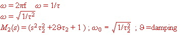
This standardization has been made , to get an fast overlook what the transfer in a bode plot will
be. Now, one may get confused with the definition of active filter-blocks. Active filter blocks are used to solve the roots of catalogued filters to be realized with similar circuits too. But as the goal
of active filter blocks differs, their spelling is different. Active analog filters using OP-AMP’s are
realized by means of active filter blocks similar to regulator blocks. To realize active analog filters, the main filter block is a second order equation and is written as follows:![]() We see, it is the same equation as the transfer of the second
order regulator block. The active filter block is written in the likeness of zeros (numerator) and Poles ((denomonator
We see, it is the same equation as the transfer of the second
order regulator block. The active filter block is written in the likeness of zeros (numerator) and Poles ((denomonator![]() ) The total definition of an active filter block is:
) The total definition of an active filter block is:
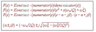 |
In this equations, normalized frequencies are used : .
.
The poles, zeros and constants must found be anywhere in a filter program or an filter catologue
.The two poles in the denominator, always must be a Hurwitz polynom, that means they are located on the 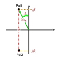 left side of the complex diagram.Fig.1 The Quality of the poles is
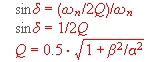
Fig.1 Poles of second order denominator in a complex diagram
To realize different kinds of filters, following formulas are used : ( Equation of only one circuit of n total circuits)
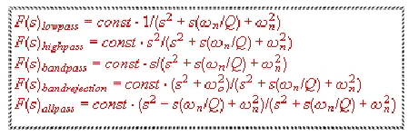 |
The total placement of poles and zeros for the different filter types are shown in Fig.2
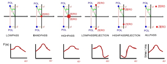 |
Fig.2 Poles and Zeros for different filter types
A high grade filter may have n numbers of the shown poles and zeros which must be realized by means of OP-AMP circuits.
This explanations of active Filter blocks was written to explain the difference between regulator blocks and active filter blocks. How to select poles and zeros in catalogue and to realize filter circuits can be found elsewhere or in following readings:
- Active RC-Filter ......?search
- H.Aisenbray,L.Gohm, H.Griesinger,”Ein allgemeines Verfahren zur Synthese aktiver RC -Filter”AEG-Telefunken 1970
- “Aktive Filters”, McGraw-Hill 1970
- Bruton, “RC aktive Circuits”Prentice Hall 1980
- Saal, “ Handbuch zum Filterentwurf”AEG-Telefunken