|
Lechler’s Website: |
|||||||
|
|
|||||||
|
|
|||||||
 |
||||||||||||||||||||||||||
|
Engineering - Electronics - Content : |
||||||||||||||||||||||||||
|
Electronic Power Supply ,Switchers, Converters and low frequency Circuits, Content:
|
||||||||||||||||||||||||||
|
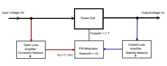
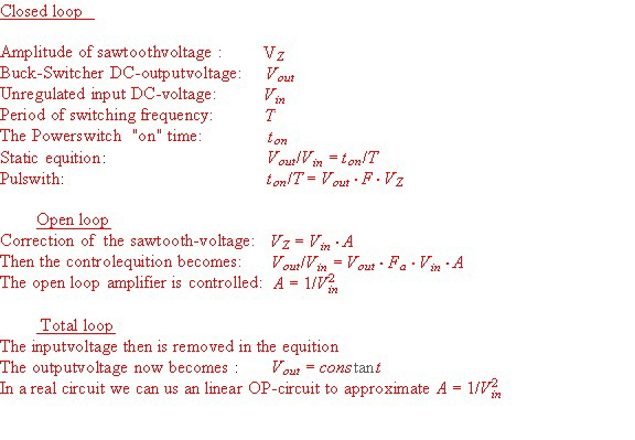
Open loop for Switching regulators for power supplys : German Patent DE3609731 The closed loop stability of switching regulators is not easy to get. Especially if the stability requirement of the output voltage is below 1%. One can overcome this problem by using an open loop, witch controls then the most of the output voltage deviations. This then allows to reduce the feedback gain at a value below ringing of the loop. Figure 1 shows the circuit of a typical switcher with a closed- loop-amplifier F including stability networks, current feedback and circuits. The pulswith is produced by means of a saw tooth voltage having an amplitude of Vz. The amplitude of this saw tooth voltage now is controlled from the input voltage via a correction amplifier A. The result is a constant output voltage, even without a closed loop. The closed loop gain can be reduced and stability problems are minimized. Figure 1 Switching regulator with open loop
|
||||||||||||||||||||||||||
|
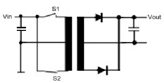
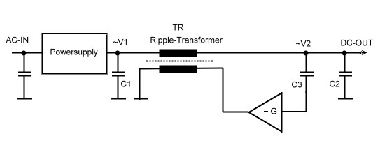
Ripple-regulator reduces bus ripple without electrolytes. Electrolytes are the big reliability problem in power conditioners. If the frequency of the produced ripple is high enough to be filtered with plastic-capacitors, the problem is solved. But in some cases, this capacitors are to big and/or not useful at higher temperatures. A ripple regulator may be solve this problem. The ripple regulator is a voltage regulator working only from the AC on the output bus. The feedback must therefore be fast enough to regulate the ripple to minimum. A switching or big analogue-transistor is not necessary to run a ripple regulator. A little transformer driven by a small transistor, will do the job. If the inrush current of the to the output is controlled, a very small transistor can be used too. C1 and C2 are SMD-high frequency de-spiking capacitors. The loop of the feedback must be fast enough to regulate the ripple frequency. A feedback network has to be used to ensure stability. Fig. 1 shows a tested circuit for a 3A/12V-switcher having an output-ripple of 20 kHz. The ripple was reduced by a factor of 500 using a E16 high my-core.The same circuit can reduce 50 Hz ripple from simple power-supply’s without big ripple-capacitors .The ripple transformer then becomes relatively large, but can encounter very high temperatures. Fig. 1 Ripple-regulator |
||||||||||||||||||||||||||
|
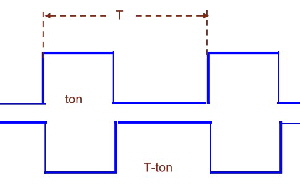
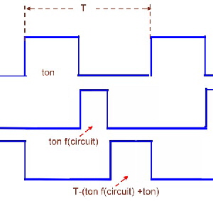
Fast switcher power cells FSC for communication power supply’s, (FSC= fast switcher circuit) A new generation of power supply switchers is presented. This switchers are based on the electronic programming of several pulses to switch power switches on and off. The function of the programming is mathematically correlated to requirements of a power-cell. The basic function is explained in Fig.1 showing the difference between regular power switches as buck, buck boost , boost or enable .The regular switcher has on and off time where the mathematical relation between both is simple only the difference between both ,whereas the sum of both times is the switcher period. The FSA switcher has tree switches and tree switching times. The sum of the three times is the switcher period . The three times are somehow programmed mathematically by an equation or by means of an electronic device. Fig.1 Usual switcher timing Fig.2 New switcher timing ####
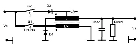
To get such a switcher run, we must first find a circuit which combines
the classical buck and the boost mode.The result is shown in Fig.2 The Function is as follows: We find 2 electronic switches, S1 and S2. S1 closed, led the charging current I1 flow through L/x. S1 open and S2
closed is the boost discharging mode .The coil de charging current from L/y is I2 . The energy in the inductor is added to
the battery voltage and we get Va > Uo. If both switches are open , the de-charging is continued from L via D1 and I3.
This is equivalent to the Buck mode and we get Ua<Uo. In a balanced condition where the regulator feedback is closed, the coil will never be discharged completely . Now we lo Fig.2 The FSC buck boost regulator
A simple mathematical relation is a factor k. Then we get the following simple time relations:
Fig.3 Balanced coil current
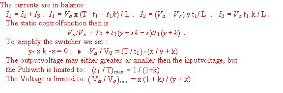
Fig.4 static equations If we want watch the dynamic behaviour, we decrease the control pulse t1 very hard with a negative time jump
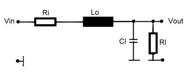
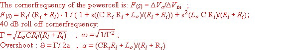
This result shows , that the new power cell is very fast reacting to distortions, that means, that the closed loop will counteract very fast too load jumps as it my happen in a communication system using switched power amplifier channels .Under this conditions, a slow switcher regulator my produce dangerous voltage overshoots. By means of the inductance Lo , we can certain the analogue regulator control circuit of Fig.9 which is a normal low pass as usual . Vin here is the input feedback voltage to compute F(s), not the DC input.
Fig.8 Computing corner frequency and roll off
This power cell is only one example of dozens of possible new switcher cells which are possible especially if the factor k is made nonlinear by means of an OPAMP: Fast buck boost switcher regulator cell #1 If the primary coil of a conventional buck boost switcher is tapped, we get the circuit of Fig: 9.
If we make:
we get:
This means, the new circuit is faster than the common circuit! Fast switcher buck regulator Cell #9 If the coil of a conventioal buck switcher is tapped, we get the circuit of Fig:10
If we make:
we get:
The fast buck switcher regulator Cell #13 If the coil of a conventional buck switcher is tapped and transformed, we get the circuit of Fig:10
If we make:
we get:
If we make:
we get:
The fast buck boost switcher regulator Cell #14 Tapping the common buck boost switcher cell leads to Fig 11:
we get:
The fast boost switcher regulator Cell #15 Tapping the common boost switcher cell leads to Fig 12
If we make:
we get:
The fast boost switcher regulator Cell with energy-back-flow #16 The common buck switcher cell with tapped secondary winding leads to Fig 13
If we make:
we get:
A fast switcher regulator Cell with energy-back-flow #17 A new switcher cell with energie feedback leads to Fig 13
If we make:
we get:
The efficiency optimized fast switcher regulator Cell #24 A new switcher cell working only in the upper output-voltage range, leads to Fig 14
If we make:
we get:
T he fast switcher regulator Cell having controlled loading and controlled deloading #36 Working with 4 switsches to control charching and discharching time, Fig.15
we get:
T he fast switcher push pull regulator Cell #32 Working with 4 switches in a push pull boost converter give high current on the output Fig.16
If we make:
In the similar manner, the shown circuits may be modified to a push pull converter. |
||||||||||||||||||||||||||
|
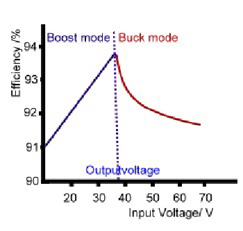
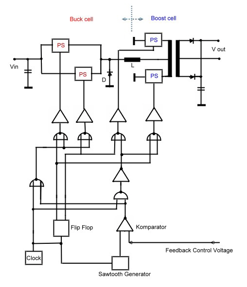
Combine buck and boost power cells, to optimize efficiency. German Patent DE 2941 009 C2 Wide regulation switchers, have the problem of low efficiency at the end of the input voltage range.This decrease can be up to 10 % of the maximum efficiency. The combination of different power cells can overcome this problem. If for instance a boost cell runs at the lower values of the input voltage range, and the buck mode runs at the lower input voltage, one can get an efficiency as Fig.1 shows. But combining two different cell types may be a problem. I propose to combine the cells by means of the electronic control circuitry. If we divide the saw tooth voltage of the puls modulating circuit in two parts , switching the clock frequency between buck and boost mode, the power mode will automatically change at the midst of the input voltage range.The circuit is shown at Fig.2. We see the 2 buck switches directly connected to the voltage input. The boost switches are connected to the output transformer. The coil L is used in both modes. D is the free-wheel diode necessary in the buck mode.The two boost transistors act as push pull switches for the transformer. In the boost mode, the switches are both in the on condition, what cancels the transformer off. The buck switches are saturated and the coil L is charged with the input voltage.The clock is divided using a toggle flip flop to drive the different cells via NOR logic devices.
Fig.2 Logical circuit, combining buck and boost cells.
|
||||||||||||||||||||||||||
|
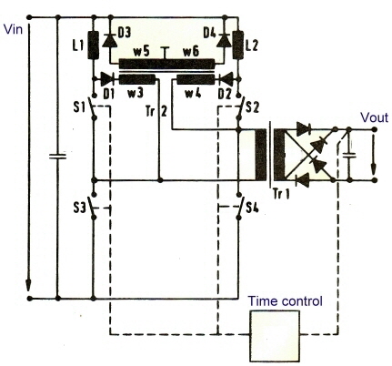
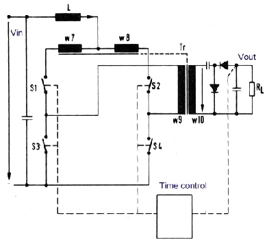
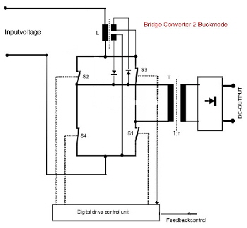
Regulated High Voltage DC Converter has low output ripple . German Patent DE 4302598 C2 Normally, a regulated DC Converter is controlled changing the duty cycle between inductor charging and discharging mode. During the charging mode of the coil, the energy on the output is derived from an energy storage capacitor.This usual way of regulating, leads to a certain amount of ripple on the output voltage. In low output voltage converters, this ripple can be easily reduced . But if the output voltage is in the kV-range, the ripple filters are voluminous and unreliable. A bridge converter power cell, can be modified to work as pumping converter controlled from a duty cycle change, whereas the output duty cycle is constant. Excessive energy in a charging inductor is pumped back to the input voltage source. In using this circuit, the ripples on the output are reduced to very small spikes even during primary duty cycle variations. An other advantage is the increase of the feedback control speed, because no ripple must be filtered out in the loop circuitry. Lets look first to the circuit of the bridge converter at Fig1. We have the output transformer
We have the output transformer Tr1, the switches S1, S2, S3, S4, and the energy back transformer Tr2 and two pumping coils L1 and L2. The switches S3 and S4 are periodically switched with a duty cycle of 1:1, whereas the switches S1 and S2 get time variation control pulses. Fig.2. They switch the load via the transformer Tr.1 during charging and de-charging of the coils, that means energy is transferred to the output at the time where energy is pumped from and back of the source Vin. .
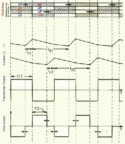
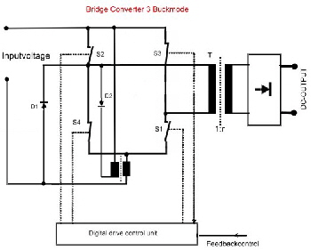
Fig.2 Bridge converter drive diagram Combine push pull and bridge converter as pulswith regulator. As the regulated pumping bridge converter of the above circuit needs a lot of components , I try to simplify this bridge converter into a combination of bridge and push pull converter. The output transformer will have two more windings having less turns then the main primary winding. If we change the power switches between the different primary windings, we get a buck boost converter with tree different charging times of a energy storage coil L. The result is the same as above, constant duty cycle for the output voltage. Fig.1 shows the circuit. The switch timing is somewhat different from Fig.2. If I will find the time, the timing of the switches will be calculated and the time to voltage control formula from the balanced currents in the coil L shown.
Fig.3 Regulated Push pull bridge converter
|
||||||||||||||||||||||||||
|
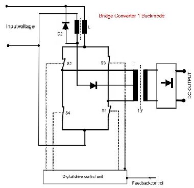
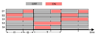
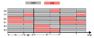
Regulated DC-Bridge Converters in Buck Mode. German Patent DE 3808432 C1 Classical Bridge DC to DC Converters are not regulated. But due of their four switches, they are excellent configurations to be pulswith regulated in many configurations. Sure an energy inductance is necessary, where the energy is stored stored , transformed and somehow brought back into the current cycles. Either back to the battery or to the output. If it pumped to the output there are two possibilities, either the coil energy is added as parallel current (buck-mode) or added as series voltage (boost-mode). Here are three pulswith controlled Bridge Converter Circuits which work in the buck mode. Fig.1 shows a controlled bridge converter with center tapped output transformer, where the buck current flows from the energie storage coil L via D2. D2 only is a de-spiking diode. The output voltage equation is the same as in a conventional buck free-wheel converter: Uout / Uin = (ton / T) r ; Fig.2 shows the switching diagram. It is obvious, that the transformer is periodically switched to the input voltage via S1 / S2 and S3/S4. During this time, L is loaded. The discharging of the Coil then comes in the push pull mode versus S1 and S3.
Fig.2 Switch drive of the regulated bridge converter 1
An other circuit is shown at Fig.3. Here are the push pull windings on the storage coil, not on the transformer.This simplifies the transformer . In doing so, the digital drive must be different. Fig.4 In an other circuit, the complexity of transformer and coil is reduced, using the primary winding of the transformer T for energy injection by means of better circuitry. Fig5 In this circuit, the same digital drive as in Fig.2 is valid. S1 and S4 are used, to switch the discharge energie of the coil into the the output transformer.
Fig.4 Digital drive of Fig.2 and 5
Fig.3 Buck regulated Bridge converter 2 Fig.5 Simplified buck regulated bridge converter 3.
|
||||||||||||||||||||||||||
 ok to the Current trough the inductance during the whole cycle.
Fig.3
ok to the Current trough the inductance during the whole cycle.
Fig.3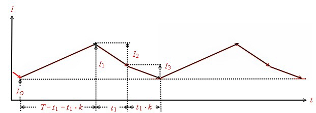


|
|||||||||||||||||||||||||||||||||||||||||||||||||||||||||||||||||||||||||||||||||||||||||||||||||||||||
|
Electronischer Brückenwandler arbeitet als Aufsteller German Patent DE 3808433 Zur Versorgung von Mikrowellenröhren mit Hochsannung wird üblicherweise ein DC- Wandler verwendet.Iin dessen Transformator wird die Versorgungspannung der Röhre auf die notwendige Höhe transformiert. Für kleine Geräte mit Miniaturtranformatoren wird dies bei Spannungen über 3kV wegen der notwendigen Isolation schwierig. Wenn der Wandler zusätzlich im Boostmode arbeitet ,kann der Ausgangstransformator wesentlich kleiner werden; da die Primärspannung grösser ist. In Fig. 1 ist ein Brücken-Wandler der als Boostegler arbeitet, .und dessen Ansteuerung gezeigt, Fig.2 zeigt den notwendigen Steuertakt. Während der Brückenwandler mit S3 -S5 normal im Gegentakt arbeitet, arbeitet S1 in jedem Brückentakt als pulsbreiten geregelter Boostschalter. Electronic Bridge Converter works as Boost Regulator, To supply microwave tubes with their working voltages, a high-voltage DC converter is used. It is common to transform the supply voltage of the tube in the converter’s transformator to the necessary height. For small devices with miniature transformers, this is difficult at voltages above 3 kV because of the necessary insulation .When the converter is operating in boost mode, the output transformer can be much smaller. In Fig. 1, a converter bridge converter and its control is shown, which works as a boost regulator. Fig.2 shows the necessary control clock sequence. While bridge converter with S3-S5 is normal working in push-pull mode, works S1 in each bridge Phase as pulse width controlled boost switch.
Fig.1,2 Bridge Converter-Boost-regulator / Brückenwandler als Hochsteller
|
|||||||||||||||||||||||||||||||||||||||||||||||||||||||||||||||||||||||||||||||||||||||||||||||||||||||
|
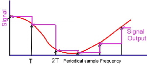
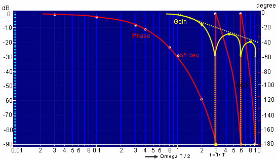
Transmission of Sample and Hold As it is well known, a sample and hold takes signal probes and keeps the amplitude of this probe constant until the next sample peak. Fig.1 To use this circuit in a feedback of a power supply, one has to know the amount of negative phase the sample and hold will produce in a loop. As the S+H is periodically switched, periodically Phase jumps of 180 degree appear at the multiple of the sample frequency. Fig.2 Whereas the Gain has a slope of -20 dB / Dec.
Fig.2 S+H Gain and Phase
|
|||||||||||||||||||||||||||||||||||||||||||||||||||||||||||||||||||||||||||||||||||||||||||||||||||||||
|
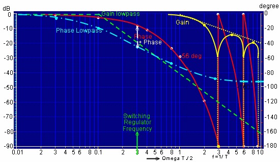
Sample and Hold improves Switcher Loop. Feedback loops in general , in power supplies or some other analogue regulation loops, must be cleaned from ripples, fast distortions and short time disturbances. This is not really part of the necessary system loop, but an important part for the electronic loop circuits . Normally little low passes or integrator circuits are used to cut the ripples off. But this circuits will produce negative phases up to 90 degree in a loop and deteriorate loop quality. To avoid this negative phase, a sample and hold can be used instead. Sure the sample and hold produces negative phase too, but the total loop phase will shown an improved loop condition. Regulation using Sample and Hold in the Feedback and digital software is called DDC (Direct Digital Control), but in this application, the sample and hold is used in the analogue feedback part of a switcher power supply loop. If the sampling frequency is chosen to be 10 times the power supply ripple frequency, the negative phase in the loop due of S+H may be only -10 degree. The saving of Phase due of the S+H, can improve the stability of the regulator and its reaction speed.. Example: A switching regulator output has 500 mV ripple. After dividing it with a resistor loop divider, the ripple is 250mV. The circuit sensitivity of the regulator is limited due of gain and latching effects, to 20 mV. Necessary damping of the ripple d = 20dB. A 20 dB first Order low pass is useful to damp this ripple. The green lines of Fig.1 shows the gain and the phase of this low pass. The additional negative phase for the loop is 10 to 40 degree.(green) Using a sample and hold instead of a low pass, the ripple becomes almost zero and the negative phase will be only 0 to 10 degree due of sample and hold (Red). This makes it possible, to make the regulator 5 times faster if using a sample and hold in the loop. Fig. 1 First order low pass compared with a sample and hold
Example of a buck-regulator with sample + hold in the loop. Fig.2 shows the block diagram of a switching regulator having a simple and hold in the loop. The numbers of blocks are.
Without 5 and 6 the circuitry is the same as a normal switcher circuit. The sample and Hold is synchronized from the Power switches frequencys sawtooth. Fig.3 shows Gain and Phases of the single devices and the total loop. The S+H frequency is 10 times the clock frequency to prevent spikes. At least, is the loop very faster as a normal switcher loop and has a better stability.
Fig.2 Switching-regulator with Sample and Hold
Fig.3 Open loop Bode plot of Fig.2
Example of a buck-boost regulator, with sampler in the loop; German Patent DE 3328840 C2 We have seen above, that the low pass in the loop which eliminates the ripple from the output-voltage makes the stability problem in switcher regulators due of producing up to 90 degree of negative phase. Above we used a standard sample and hold circuit to overcome this problem. An other way is, to sample the output voltage and build a pulswith-modulator controlled from this output voltage. Fig.4 shows the circuit of a buck boost regulator. In this circuit the comparison sawtooth voltage is sampled and renewed by means of an integrator and two comparators establishing the Power transistor to control the Power transistor.
Fig.4 Buck-Boost regulator with sampled sawtooth
Example of switching regulators, with high grade inputfilter; German Patent DE 2950340 C2 The ripple filter loop problem can be solved the conservative way, increasing the filters grade to match the phase to the switchers data. If the filter has the form of,
There are many ways to realise the filter, on way is shown in Fig.6 : Loop filter circuit
As an Example, the open loop of a buck switcher having the filter of fig 6 in the loop is Fig.7 : Total switcher loop
|
|||||||||||||||||||||||||||||||||||||||||||||||||||||||||||||||||||||||||||||||||||||||||||||||||||||||
|
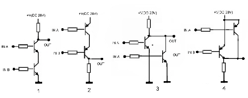
RTL-Logic improves reliability in Power Supply’s Power supply's sometimes need logic circuits. Of course at low voltage supply’s, we use the customary IC’s. But for high Voltage supply’s sometimes is it more reliable to use simple RTL logic and make their circuit a direct part of the Power supply circuit. Here are a few classic RTL circuits to improve the reliability of Power supply’s for traffic or space applications. Fig.1 Classical RTL logic circuits
Simple DC-Circuit improves TWT live-time. German Patent 1566020 The TWT (Traveling Wave Tube) is the last tube of the electronic tubes family are still in use. It is required to
build high power GHz transmitters with low distortion. But their draw back is the decrease in power output over
the life due to a reduced electron beam. Using a resistor and a feedback circuit we can compensate the decrease
of RF- Power. Fig. 1 shows a diagram of a simplified TWT and its P The Grid 1 Voltage then becomes a function of tube lifetime, ad electron emission is regulated. VG1sum=Vg1+V(f(Jc(live of tube)))
Fig.1 TWTA Circuit using Grid feedback.
TWTA preheating time is made proportional to power interrupting time. Simple Circuit can measure main power interrupting failure without an auxiliary battery. German Patent DE 3332940 C1 High-power transmitters TWTA's still have a tube that must be preheated after switching on. This preheating time normally is about 3 to 10 minutes. This is a problem in case of short main power interrupting failure in the seconds range. In this case ,a preheating time of 5 minutes is unnecessary, but the preheating time should be : Tfilament =tfailure* Tpower. To realize this ,the main power interrupting time must be measured. Normally one would use a digital timer supplied by a battery, to measure this time. But then, due of the battery, the reliability of the TWTA becomes low. The question is, can we measure the main power interrupting time without the use of a battery? The solution is: The trick is the use of a dual slope integrator using a plastic capacitor C1 in the feedback. See the circuit of Countersign regular condition, C1 is charged and the relay Rel =on. In case of main power failure, Rel = off, C1 discharges over R4, R5, see Vc. After that when the main- power is on again, C1 is charged again. Using Comparator K1, the level of discharged C1 voltage becomes a measure of the power interrupting time. See Fig.2 If the time constants of C1 and the comparator K1 level is used properly, the output of K1 can directly switch on the preheating process of the TWTA.
|
|||||||||||||||||||||||||||||||||||||||||||||||||||||||||||||||||||||||||||||||||||||||||||||||||||||||
|
How to build a fail save DC- Switch Single transistor DC-power electronic switches my fail, and stop the car, the
train or their control circuitry during traffic control. This may lead to terrible events.
Fig.1 Quad DC.switch
|
|||||||||||||||||||||||||||||||||||||||||||||||||||||||||||||||||||||||||||||||||||||||||||||||||||||||
|
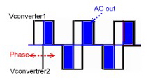
A Phase regulated high power DC-Converter needs smaller power-transistors Phase regulation in a DC Converter is a practical and helpful method to distribute the input DC Power in into paralleled DC-Converters, consisting of small and cheap switching transistors. Such regulated DC converters have a very high efficiency because, the used unregulated push pull converters can have an optimal eta of > 95% . Fig.1 shoes a block diagram of a phase regulated 2kW-DC-Converter, using two standard push pull converters, where the drive voltages of the power switches are shifted in phase as function of the feedback-control-voltage. The Square wave voltages of the converters are added by means of a power transformer. Fig.2 shows the output AC voltage (blue). The DC-Voltage, must be stored in a buck switcher L-C-Diode circuit. This circuit will decrease the efficiency a few percent. Total efficiency is about 93%: The buck storage formula is valid there, but due of the voltage adding, the ripple frequency is twice the converter frequency, which eases ripple filtering. The phase control is easy to realize, using standard logic circuitry. One converter is driven directly from the square wave clock. This Clock produces a saw tooth too. The control DC- Voltage and the saw tooth create a pulswith controlled voltage , which triggers a toggle flip flop which creates a new phase depended 1:1 square wave Fig.1 Phase regulated DC- Converter Fig.2 AC-Output voltage
|
|||||||||||||||||||||||||||||||||||||||||||||||||||||||||||||||||||||||||||||||||||||||||||||||||||||||
|
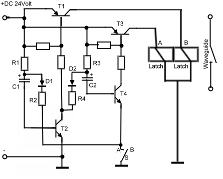
A high Power Latching Relays Driver for Wave-guide Switches. German Patent DE3040806 C2 Latching Relays come out in different sizes, they have two switching magnets, which changes status by means of two coils. Two change the status a short time drive current must be flow through one of the status coils. In case of a system voltage loss, latching relays keep its position, without any power. There fore, they are a good solution to replace storage elements in electronic equipments to prevent standby power. Small latching relays can be driven directly from an triggered mono stable Integrated Circuit. In case of a bigger Relay, driver transistors are necessary. To prevent a separate power supply in 12/24/48 Volt circuits, to feed the Integrated circuits, the latching relays driver transistor can be used to produce a switching impulse. Fig 1 shows a driver circuit used to switch a 24 Volt Wave-guide latching switch. This driver is very robust and may be used in traffic electronics too. It had been used manifold in high power TWTA’s.
Fig.1 Wave-guide Latching relays driver To change the Relays status from A to B, the switch S is set to B. The de-charging path R2 of C1 then is opened and C1 is recharged via the Base of T2. Due of this, the relay goes to B and the shorted T2 de-charges C2 and opens T4, blocking T3 and A. In case S is on A, the function is vice versa. To prevent malfunction at higher temperatures, the leakage current of C1/C2 must be kept low.
|
|||||||||||||||||||||||||||||||||||||||||||||||||||||||||||||||||||||||||||||||||||||||||||||||||||||||
|
How to regulate the classical push pull converter The circuit of the classical push pull converter using two switches and a transformer is almost 60 Years old and still used today. Fig1. remembers the function: Two Power switches S1 and S2 have the push pull modes on and off and drive a transformer with a rectangle power . A simple coil improves it to a normal boost regulator if we overlap the two switches for a variable short time. during this time, where both switches are on the transformer is canceled, and an inductance is loaded on the input voltage. Its energy is added to the output during the push pull mode. Fig.1 Classical push pull converter. Fig.2 regulated push pull converter
ratio, Lcu, Rcu To compute the values of the boost components, the outputcapacitor must be the series connection of transformer datas (Rcu + Lcu + Cload ) transformed with ratio(SQR) |
|||||||||||||||||||||||||||||||||||||||||||||||||||||||||||||||||||||||||||||||||||||||||||||||||||||||
|
The Frequency behaviour of the Power Supply Boost Switcher Power Cell Due of its simplicity and its very high efficiency of almost 100 % , the original boost switcher is very popular. But the closed loop behaviour is not as easy . To realize it in a high gain loop, some circuitry is necessary to get stability. First is to know the analogue transmission behavior of the boost power cell of Fig.1. The control transmission is the path of the pulswith ton / T to the output voltage Vout. As the feedback control loop is analogue, we must find a analogue model for the power cell feedback transmission. As the equations at Fig.2 shows the control transmission is depending on the working point of the power cell, that means the input voltage value. The given transmission formula can be directly used in an analogue bode consideration as F(s) using Fig.3. What we find here is at least a roll off of -20 dB and a damping factor which is important for stability depending on all components. That means to get the switcher stable, the values of all components must be proper selected. Further it is obvious, that the losses of the charging capacitor produce a positive loop phase. Therefore the capacitor loss stray values, must be carefully watched. Fig.1 Booster power cell
Fig.2 Equations of the booster |
|||||||||||||||||||||||||||||||||||||||||||||||||||||||||||||||||||||||||||||||||||||||||||||||||||||||
|
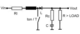
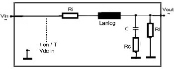
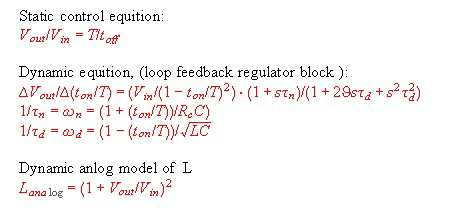
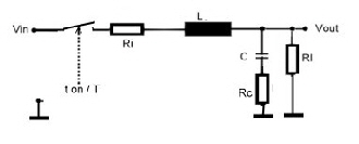
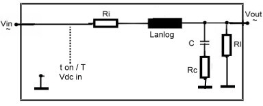
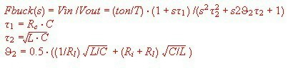
The Frequency behaviour of the Power Supply Buck Switcher Power Cell The most used power supply switcher cell is the buck switcher. This circuit is simple and robust, and so is the frequency behavior if used in a feedback loop. Link to feedback formulas The well known buck switcher cell circuit is shown at Fig.1. The power switch is continuously switched on during the on time ton. The Question now is, what will happen, if ton varies a small amount at different frequencies. A balance current consideration leads to the result of Fig.2. which indicates, the regulator block of the buck cell is a low pass equal to the switcher circuit of Fig.1. having a steady state pulswith ton / T and Lanalog = L, see Fig.3
Fig.1 Classical Buck Power cell Fig.3 Analogue Regulator block of Buck cell
Fig.2 Loop frequency behavior of the Buck cell
|
|||||||||||||||||||||||||||||||||||||||||||||||||||||||||||||||||||||||||||||||||||||||||||||||||||||||
|
DC-Wandler Einschaltstromstoß ist angepasst an die Transistor second breakdown spec..
Die Hochspannung zur Versorgung von Mikrowellenröhren z.B. Wanderfeldröhren wird aus Platz und Gewichtsgründen in Transistor DC-Wandlern erzeugt. Die Schalttransistoren der Wandler sind meist bidirektionale Transistoren. Solch ein Wandler ist in Fig.1 gezeigt. Die Leistungstransistoren sind #10,11. Beim Einschalten der Versorgungsgleichspannung ,durch den Schalter #13, muss der Wandler zwei gegensätzliche Bedingungen *1 und *2 erfüllen.
Diese zwei Bedingungen, können nur mit einem Kompromiss gelöst werden. Fig.1 zeigt einen Wandler, in dem ein Kompromiss zwischen *1 und *2 realisiert ist. Die Komponenten #10,11,12,20,21,15,16,17, stellen den eigentlichen Wandler dar. Um die Bedingung *1 zu erfüllen, wird der Einschaltgsstrom-stoß hart begrenzt, und zwar mit der Schleife der Komponenten #31,32,33. #32,33 sind die Verstärker der Konstantstrom-schleife. Um die Bedingung *2 zu erfüllen wird der Einschaltstromstoß zeitabhängig geschaltet. #45,41,48. Der Einschaltspannungsstoss durch #13 wird mit dem Komparator #40 auf Elektronik-level gebracht. Zeitverzögert, durch das Monoflop #41, wird die Höhe des begrenzten Einschsltstromtoßes umgeschaltet,Fig.4 so das eine Anpassung an die Seond-Breakdown-kurve der Leistungstransistoren erfolgt Fig.3.dadurch erfolgt dann ein schneller Anstieg der Ausgangsspannung. Fig.2 The high voltages to supply microwave tubes for instance, Traveling wave tubes, is generated from space and weight reasons in transistor DC converters. The switching transistors of the converter are often bidirectional transistors. Such a converter is shown in Fig.1. the power transistors are # 10.11. When the supply DC voltage by the switch # 13 is switched on, the converter has to fulfill two the two opposing condition's and *2
This opposing requirements can only be solved by means of a compromise. Fig.1 shows a converter which realizes a compromise between requirement *1 and *2. The components # 10,11,12,20,21,15,16,17, represent the actual converter. In order to satisfy the condition * 1, the Inrush-current is hard limited, with the loop of the components # 31 , 32.33. # 32.33 are the amplifiers of the constant current loop. In order to satisfy the condition * 2 the inrush current level is time-dependent changed. # 45,41,48. The Inrush-current through # 13 is brought on electronic level with the comparator # 40th. By means of a Time delay, by the one-shot # 41, the height of the limited inrush-current s is switched, (Fig.4) so that an adaptation to the Second -Breakdown-curve of the power transistors occurs: Fig.3, what leads then to a rapid increase of the output voltage Ua. Fig.2 Fig.1 DC-Converter with Second Breakdown matched inrush-current / Fig1 DC-Wandler mit an Second-Breakdown angepastem Einschaltstromstoß
|
|||||||||||||||||||||||||||||||||||||||||||||||||||||||||||||||||||||||||||||||||||||||||||||||||||||||
|
Literature, readings: Power supply , switcher, electronic power conditioning, Netzteile
|
|||||||||||||||||||||||||||||||||||||||||||||||||||||||||||||||||||||||||||||||||||||||||||||||||||||||
|
British , American and German Wires at a Glance Power-supply’s have Transformers and Transformers have Wires. The following tables, show British , American and German Wires:
|
|||||||||||||||||||||||||||||||||||||||||||||||||||||||||||||||||||||||||||||||||||||||||||||||||||||||


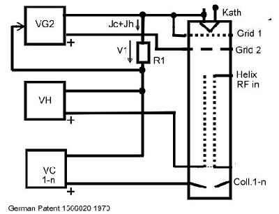 ower Conditioning. The grid 1 voltage sets
the operating point of the TWT and its output power. If the cathode emission decreases
during live-time, the collector current IC(1-n) will become smaller. Now, this current is measured by a resistor and fed back as a
voltage to the power supply grid 1.
ower Conditioning. The grid 1 voltage sets
the operating point of the TWT and its output power. If the cathode emission decreases
during live-time, the collector current IC(1-n) will become smaller. Now, this current is measured by a resistor and fed back as a
voltage to the power supply grid 1.
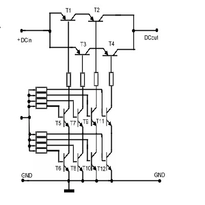 To prevent such live important failures, the single transistor switch
may be replaced by an quad switch, designed for space applications. Quad means, we use two
power transistors in series and the same arrangement as an paralleled path. So we have
four useful transistors. See Fig.1. This design is redundant for short and open failure. To drive
the bases of the power switches, we use transistor series circuits too. Now wee see, at
least two transistors must fail to get malfunction .The control voltage must be able, to supply 7
transistors bases even in case of base breakdown. As I have designed this switch in
the seventies npn transistors have been used, but as this is only an example of redundant circuitry,
modern MOS devices may be used instead, but high reliability only comes from discrete components.
To prevent such live important failures, the single transistor switch
may be replaced by an quad switch, designed for space applications. Quad means, we use two
power transistors in series and the same arrangement as an paralleled path. So we have
four useful transistors. See Fig.1. This design is redundant for short and open failure. To drive
the bases of the power switches, we use transistor series circuits too. Now wee see, at
least two transistors must fail to get malfunction .The control voltage must be able, to supply 7
transistors bases even in case of base breakdown. As I have designed this switch in
the seventies npn transistors have been used, but as this is only an example of redundant circuitry,
modern MOS devices may be used instead, but high reliability only comes from discrete components.